Introduction
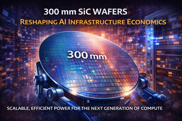
Today’s technology news reports a significant semiconductor milestone as Wolfspeed announced the successful production of 300 mm silicon carbide (SiC) wafers, a development expected to dramatically improve scalability and performance for AI infrastructure, advanced power electronics, and emerging AR/VR systems. The breakthrough was widely covered in Wolfspeed’s press release and corroborated by reporting that highlighted its strategic implications for next-generation computing platforms. This shift marks a new phase in how compute, power, and thermal challenges are addressed in infrastructure critical to the AI economy. (investor.wolfspeed.com)
Why It Matters Now
The disruption lies in expanding the manufacturing scale and capability of silicon carbide beyond legacy wafer sizes. Larger 300 mm SiC wafers increase yield potential, reduce cost per unit area, and enable integration into high-performance systems that power data centers, electric vehicles, and immersive computing. As AI workloads grow and demand more power and thermal efficiency, these materials and fabrication advance directly influences the economics and feasibility of next-generation infrastructure. (investor.wolfspeed.com)
Call-Out
Expanded SiC wafer scale unlocks scalable power and performance for AI and beyond.
Business Implications
For cloud providers and hyperscalers, the ability to source 300 mm SiC wafers offers a path to more efficient power electronics and cooling subsystems, reducing operational expenses and improving uptime. Hardware vendors can design more compact, energy-dense modules that support sustained AI training and inference demands. Traditional silicon limits are being challenged, forcing infrastructure designers to reassess materials strategies and partnerships with SiC foundries.
Automotive, AR/VR, and industrial sectors stand to benefit as well, as SiC is increasingly used in motor drives, high-voltage power electronics, and compact thermal management systems. Suppliers and original equipment manufacturers may face supply chain pressures as demand for larger SiC wafers accelerates, potentially reshaping competitive dynamics in materials and advanced packaging. (Wolfspeed)
Looking Ahead
In the near term, pilot production and qualification cycles will determine how quickly 300 mm SiC wafers enter mainstream supply chains. Over the longer term, the ability to scale production and improve defect rates will decide whether SiC becomes a foundational material for both power and RF/optical domains in computing and communication.
This advance also intersects with broader trends such as energy-efficient AI data centers, hardware-aware model design, and national policy priorities around semiconductor independence. Countries and corporations investing in SiC infrastructure today may gain structural advantage in the global technology landscape.
The Upshot
The successful production of 300 mm SiC wafers represents a structural disruption in semiconductor materials and manufacturing. By expanding wafer scale for a class of materials critical to high-efficiency power and computing systems, this development reshapes the economics of AI infrastructure, AR/VR platforms, and advanced electronics. The future of high-performance, energy-efficient systems may be defined as much by wafer scale and materials innovation as by transistor scaling.
References
Wolfspeed achieves 300 mm SiC technology breakthrough enabling scalable platforms for AI infrastructure and advanced power devices, Jan. 13, 2026. (investor.wolfspeed.com)
Wolfspeed expands silicon carbide manufacturing to 300 mm wafers, unlocking efficiencies for AI and AR/VR systems, Jan. 13, 2026. (Wolfspeed)

Leave a comment